WeChat
0551-62629462


Hotline
0551-62629462Micro preparation, high-tech masterpiece
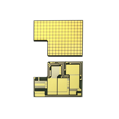
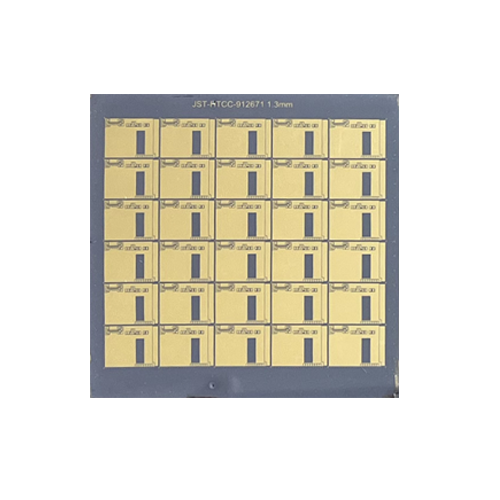
According to the different preparation principles and processes, thin film ceramic substrates can be divided into multiple unique types, among which thin film ceramic substrates (TFC) stand out for its micro preparation process. Thin film technology refers to the technique of preparing specific patterned film layers using methods such as vacuum evaporation or sputtering, photolithography and etching. The use of photolithography and etching processes results in smaller patterned feature sizes, clearer lines, and better suitability for high-density and high-frequency environments. Thin film materials and coating technology are important foundational engineering in electronic packaging engineering, mainly achieving functions such as electrical connection, component loading, special functions, and surface modification. Thin film technology endows ordinary materials with many "magical" functions, achieving the modern meaning of "turning stones into gold"
Technological advantages, helping the high-tech field
The TFC process is complex and precise, making it a brilliant gem on the crown of industrial technology. Traditional thin film processes go through dozens or even hundreds of processes, and the photolithography process alone generally involves 11 major processes such as cleaning, leveling, UV exposure, film hardening, etching (corrosion), and debonding. Changes in materials, process parameters, environmental factors, and other factors in these steps will significantly affect the quality and reliability of photolithography patterns. Therefore, controlling their orderly and reliable execution is of utmost importance in TFC processes. However, the thin film ceramic substrate produced as a result has various advantages, including high reliability at various extreme temperatures, high thermal conductivity, high wiring accuracy, low dielectric loss, controllable metal layer thickness, and strong metal ceramic bonding strength. It has been widely used in radar, LED lighting, lasers, 5G communication technology, solar energy, new energy vehicles, and consumer electronics. It is a key technology in the manufacturing of micro electronic components, providing a solid foundation for the manufacturing of high-tech products
Hefei Jiusi: Technology Leading the Future
With the continuous advancement of technology, thin film technology has shown promising development prospects in various industries. ". As a practitioner and innovator in this field, Hefei Jiusi Electronic Technology Co., Ltd. will continue to invest in research and innovation, focusing on thin film metallization and high-precision graphic preparation on single-layer and multi-layer aluminum nitride ceramics, aluminum oxide ceramics, silicon carbide, diamond, quartz glass, andBeO substrate surfaces. We are committed to providing customers with high-performance, highly reliable, and cost-effective packaging solutions. The micro preparation process and multiple advantages of thin film ceramic substrates make them a treasure in the high-tech field. The company will provide excellent services through continuous innovation, inject new vitality into the electronic technology industry, and help the future vigorous development of technology

Tag: